6 Micro- and Biofluidic device fabrication
In engineering, we can use the understanding of fluid dynamics to build micro- and biofluidic devices for certain purposes. These devices and systems entail the underlying physics in often intricate ways to meet needs and objectives. Most common applications are relatable, with a huge capital market of more than $25 billion annually.
6.1 Learning Objectives
- Learn about methods of fabrication
- Discuss specific examples in the industry
6.2 Macro/conventional fabrication
Conventional fabrication usually happens on a macroscopic scale with featured sized of 1 mm or bigger. Macro fabrication deals with ordinary dimensions and the machinery takes up significant room. Examples for conventional fabrication are CNC machining, moulding, casting and extrusion.
6.3 Additive Manufacturing
Additive Manufacturing or 3D printing is a production process by which an object is produced in an additive fashion, layer-by-layer. The procedure to fabricate a 3D printed object starts with a 3D CAD (Computer-Aided Design) model which is then converted into a printable file (e.g. STL). This file then has to be processed with a slicing software which turns the 3D model into multiple layers, that the 3D printer can print, and also creates the tool path for the printer to follow. Afterwards the sliced model can be turned into a physical 3D object with additive manufacturing.
Based on the quality and type of the 3D printer featured sizes range from a few microns to 1 mm for different applications (Table 6.1).
Table 6.1: Different methods for additive manufacturing Micro/Nano Fabrication
| Method | Standard minimum resolution | Applications and product size | Materials | Cost |
| Fused Deposition Modelling (FDM) | 500 microns | Medium and large size (up to 1 m) | Thermoplastics | Low |
| Multi-jet printing | 40 microns | Medium and small size (up to 25 cm) | Thermosets | High |
| Stereolithography (SLA) | 25 microns | Medium and small size (up to 20 cm) | Thermosets | High |
| Powder Bed Fusion (e.g. SLS, SLM …) | 10 microns | Medium and small size (up to 20 cm) | Plastic, Metal | Very high |
| Two Photon 3D Printing | 1 micron | Microstructures | Thermosets | Medium |
6.4 Micro/Nano Fabrication
With the existence of macro-fabrication techniques, the question arises as to why micro or nano fabrication is needed:
- Downscaling the fabrication from macro to micro generally saves fabrication time, material, space and cost.
- By going even smaller to nanostructures new spectacular physical and chemical properties can be determined, therefore nano fabrication is needed.
Example: Graphene in nanoscale
An example for special properties on nanoscale is graphene, which is a two-dimensional sheet of carbon atoms and combines several properties, such as being very strong, but also light and flexible and highly conductive. One of those layers of graphene theoretically has a thickness of 0.345 nm.
Generally, the two basic fabrication strategies that are used are the top-down– and the bottom-up approach.
Using the top-down approach, micro/nano-scale materials are created by physically or chemically breaking down lager materials. A bulk of material is first turned into fragments which can then be broken down even further into micro/nano-scale structures.
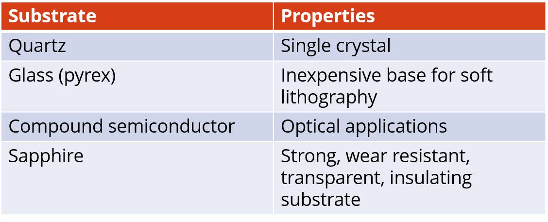
Top-down fabrication is classified based on the substrates (the surface on which the device is fabricated) that are being used. Depending on the application, following substrates can be used as shown in Table 6.2. The most common used substrate is silicone.
To perform top-down fabrication, different techniques can be used, such as photo-lithography, deposition and etching.
The implementation of photolithography can be divided into five steps (Figure 6.1):
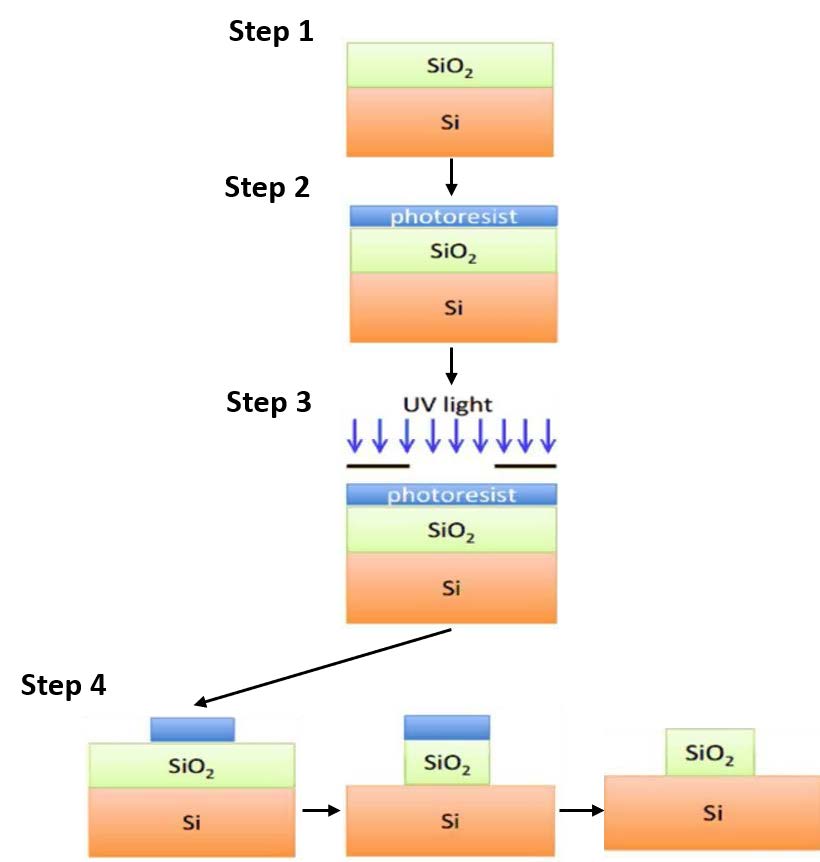
- Cleaning: Removing organic or inorganic contaminations presented on the wafer surface, which could cause problems with the photosensitive resist layer.
- Spin Coating: A photosensitive resist layer is spin coated onto the substrate (wafer). The wafer covered with a layer of photoresist is then baked in an oven.
- UV Exposure: Expose the wafer to UV exposure through a photomask, which covers those parts of the photosensitive layer, which are not supposed to harden. The photoresist either cross-links or becomes soluble.
- Developing: Developed by dissolving the exposed/unexposed resist, to now transfer patterns to the substrate. A multilayer is achieved by aligning the subsequent masks.
- Inspection and hard baking: Checking for errors and assuring durability.
If the microstructures are supposed to be embossed into soft materials, a photolithography technique called soft lithography is used. It is the process in which soft materials (e.g. PDMS) are patterned using a master mould made by photolithography. Soft lithography can be viewed as a complementary extension of photolithography.
Deposition can be classified into physical and chemical deposition:
Physical Deposition
- Material is removed from a source
- It is subsequently carried to the substrate
- Material is then dropped there.
Physical deposition includes techniques like spin casting and physical vapour deposition (PVD).
Physical vapour deposition (PVD) first heats up the source material inside of evaporator. The vaporised material is transported to substrate to create a layer of deposit material on substrate. The whole procedure is done in a vacuum chamber. Differences among PVD techniques include different methods on treating source material, transporting vaporised material and cleaning deposition.
Chemical Deposition
- Reactants are transported to the substrate
- A chemical reaction occurs
- Products deposit on the substrate to form the desired film
Techniques to perform chemical deposition include thermal oxidation, chemical vapour deposition (CVD), epitaxy and electrodeposition.
Etching is defined as the selective removal of solid material through chemical or physical reaction. It can be divided into wet etching and dry etching:
- Wet etching: A chemical method which uses a reactive solution to etch away the solid substrate. This method works either isotropic or anisotropic (crystals only).
- Dry etching: Solid substrate is etched by gaseous species (plasma method) using sputtered or dissolved with reactive ions or a vapour phase etchant. This method can be classified as RIE – reactive ion etching – and DRIE – deep reactive ion etching. This method works either isotropically or anisotropically (as determined by processes utilised).
The top-down approach is the bottom-up approach, where nano materials are self-assembled atom-by-atom or molecule-by-molecule. Single atoms join together into clusters which are then combined to form nanoscale structures
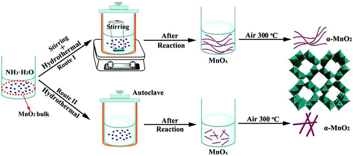
Chemical synthesis is a hydrothermal method that refers to heterogeneous reactions in aqueous media above 100 °C and 1 bar. For example, synthesis of ultralong α-MnO2 nanowires (NWs) from commercial MnO2 powders through hydrothermal treatment under magnetic stirring. Figure 6.2 shows the hydrothermal synthesis of ultralong α-MnO2 nanowires and α-MnO2 nanorods with and without stirring.
6.4.2.2 Self-assembly
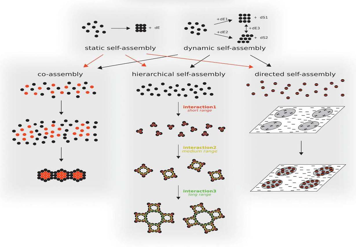
Self-assembly refers to the process by which nanoparticles or other discrete components spontaneously organise due to direct specific interactions and/or indirectly, through their environment.
Graphical rendition of static and dynamic self-assembly and how they relate to co-assembly, hierarchical assembly and directed assembly can be seen in Figure 6.3.
Top-down micro/nano-fabrication techniques create a nano-scale structure starting from a bulk volume, like photolithography. Bottom-up micro/nano-fabrication techniques create a nano-scale structure building up from atoms and molecules, like self assembly.
6.4.2 Fabrication techniques for nanodevices
Standard photolithography tools allow minimum featured sizes down to around 22 nm. Nanolithography techniques like electron beam lithography, focused ion beam, nanoimprint lithography, interferometric lithography and sphere lithography have been developed to beat the minimum size limit in standard photolithography.
Another technique used for the fabrication of polymeric nanochannels is called direct imprinting (Figure 6.2). A silicon master, which consists of micro-scale transport channels and a funnel-like inlet for the nanochannels, is filled with UV-curable resin.
![Figure 6.4: Example of the fabrication of a nanofluidic device [8]](https://oer.pressbooks.pub/app/uploads/sites/28/2020/11/nanofluidic.jpg)
6.4.4 Materials
Depending on the application, different materials are necessary to achieve certain properties. A list of common materials can be found below including why there are used and what drawbacks they bring.
- Silicone
Most used to create integrated circuits (IC) in consumer electronics. It is widely available functions perfect with electronic devices because it is nonconductive. The problem with silicone is its high cost.
- Metals
Besides using metal for the entire device, it can also be used to create MEMS elements, such as electrodes and sensors. Because they are highly conductive, they are also important for electronic applications. The problem with metal is also its high cost and that some metals can be toxic and present a health risk, when working with them.
- Polymers
Polymers are mostly used for microfluidic applications, such as cartridges for blood testing, because of the low material cost and the design freedom. Unfortunately, the machines for polymer fabrication are expensive which in turn increases fabrication cost. Additional problems involve the low resolution of polymer devices.
- Ceramics
They are applied where a combination of material properties is needed. Ceramic is a biocompatible, high temperature resistant and really strong material. Its fabrication process also allows a high design freedom. The problem with ceramics is due to their strength; they are brittle when it comes to punctual stress.
6.5 Selection of Fabrication Method
The selection of the right fabrication methods depends on various factors. It’s possible to select either by target size or method of application.
6.5.1 Target size
Depending on the necessary resolution of the object different fabrication methods have to be used (Table 5.3).
Table 6.3: Different fabrication methods depending on target size
| Resolution | Available Fabrication Methods |
| 1-100 nm |
|
| 2-10 nm | Electron-beam Lithography (EBL) |
| 30-80 nm | Optical UV lithography (D-UV, E-UV) |
| 50-100 nm | Dry etching / plasma etching |
| 1 µm | Wet etching |
| 1 µm | Photolithography |
| 30 µm | Micromachining |
| 200 µm | 3D Printing (3D Wax printing, bio-printing) |
6.5.2 Application
Depending on the application that the object has to fulfil, different methods must be applied:
| Photolithography | Make a thing/thick layer/structure over a substrate (at micron size). |
| 3D printing | Make a 3D structure at bigger scale (micron and millimetre). |
| Thin film/Deposition process | Deposit a thin layer over a substrate. |
| Etching | Etch a depth into a substrate. |
| Chemical Synthesis | Fabricate/grow nanoscale materials. |
| Soft lithography | Make a microchannel in a soft polymer. |
6.6 Coupling of Domains
The basic functionality of many devices is in coupling one domain to another, and this coupling is typically described by material properties.
Coupling of mechanical and electrical properties is done with microelectromechanical systems (MEMS). Other properties that can also be linked using coupling are electrical to thermal and thermal to fluids. The failure modes of many of these devices are in coupling one domain to another, e.g. package stress interacting with a piezo resistor.
6.7 Execution of microfabrication – Cleanrooms
Cleanrooms are used for the production or research of micro-biofluidic devices. They are designed to maintain extremely low levels of particulates, such as dust, airborne organisms, or vaporised particles. Their level of cleanliness is quantified by the number of particles per cubic meter at a predetermined molecule measure.
6.8 Packaging
Depending on the materials and the fabrication techniques, different packaging techniques are used. Important consideration when packaging devices are to make sure, that fluid connections are properly sealed. Also, the packaging has to endure required pressure and other properties of the device. Two examples and their considerations of packaging are listed as following.
Example: Packaging a microturbine
The micro-turbine device is a device featuring fluidic and electrical connections between a seal acrylic plate and die via o-rings. The considerations before exporting out the masks for this device includes pressure distortion and placement for o-rings.
Example: Packaging a pressure sensor
A monolithic pressure sensor with circuitry in a custom bipolar process mounted on silicon support mounted in plastic package. The consideration includes membrane location, sealing requirement and electrical bondings.
Packaging is an important part of micro/nano fabrication and is vital for mass production. For example, electrical and fluidic components insulation is very important when packaging a micro-turbine.
6.9 Australian National Fabrication Facility
Virtual Tour
Review Questions
Practical polymer used as soft material (Polydimethylsiloxane)
having uniform physical properties across all directions and magnitudes
Displays variation in physical properties across different directions and magnitudes